Are you a beginner looking to dive into PCB design and assembly? This ultimate guide to PCB design will walk you through the essentials, from understanding what a PCB is to the step-by-step process of creating and assembling one. Whether you’re a hobbyist tinkering with electronics or an aspiring engineer, mastering PCB design starts with grasping the basics: schematics, layout, and fabrication. By the end, you’ll have the knowledge to avoid common pitfalls and create functional boards that power everything from simple gadgets to complex devices.
In today’s rapidly evolving electronics world, the PCB market is booming. Valued at USD 70,800 million in 2025, it’s projected to reach USD 117,500 million by 2035, growing at a CAGR of 5.2%. At Panasia Solutions, with over 25 years of expertise in electronics manufacturing, we leverage global facilities and sustainable practices to help beginners and pros alike turn ideas into reliable prototypes.


What Is a PCB and Why Is It Important?
Let’s start simple. A Printed Circuit Board (PCB) is the backbone of modern electronics, connecting components like resistors, capacitors, and ICs through etched copper traces on a non-conductive substrate.
Why bother learning PCB design? In a nutshell, it allows you to customize circuits for specific needs, reducing size, cost, and errors compared to breadboarding. For beginners, it’s empowering – imagine building your own Arduino clone or IoT sensor.
Industry insights show PCBs are everywhere: in smartphones, cars, and medical devices. With miniaturization trends, PCBs are getting smaller and more complex, driving demand for skilled designers.
Over the next few topics, we’ll cover terminology, methods of assembly, and more, drawing from resources like SparkFun’s PCB basics.


Essential Tools and Software for PCB Design Beginners
Getting started with PCB design requires the right tools. For software, free options like KiCad are excellent for beginners, offering schematic capture, layout, and 3D viewing.
Other top picks include Altium Designer for pros, EAGLE (now part of Fusion 360), and EasyEDA for cloud-based ease. In 2025, AI-integrated tools like those in Altium are trending, automating routing and checks.
Hardware-wise, you’ll need a computer, multimeter, soldering iron, and perhaps a 3D printer for enclosures.
- Free vs. Paid Software: KiCad is open-source and powerful; Altium offers advanced features but at a cost.
- Learning Resources: Tutorials on YouTube or sites like Circuit Basics.
- Budget Tips: Start with free tools to build skills before investing.
These tools make the guide to PCB design accessible, even for novices.
Step-by-Step Guide to PCB Design
Ready to design your first PCB? Follow this step-by-step guide to PCB design.
- Create the Schematic: Draw your circuit diagram using software. Include all components and connections. Double-check for errors here – it’s easier to fix now.
- Component Selection: Choose parts based on specs like voltage ratings. Use libraries in your software.
- PCB Layout: Place components on the board virtually. Optimize for space, signal integrity, and heat dissipation.
- Routing Traces: Connect pins with copper traces. Follow rules: wider for power, shorter for high-speed signals.
- Add Ground Planes and Vias: Enhance stability with ground fills; use vias for multi-layer boards.
- Design Rule Check (DRC): Run software checks for clearances and errors.
- Generate Gerber Files: Export for manufacturing.
This process, as outlined in Cadence’s PCB design series, ensures a solid foundation.


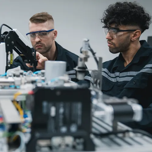
The PCB Assembly Process Explained
Once designed, it’s time for assembly. The PCB assembly process involves mounting components onto the board.
Key methods: Surface Mount Technology (SMT) for tiny parts and Through-Hole Technology (THT) for larger ones.
Steps include:
- Solder Paste Application: For SMT, apply paste via stencil.
- Pick and Place: Machines place components precisely.
- Reflow Soldering: Heat to melt paste and bond parts.
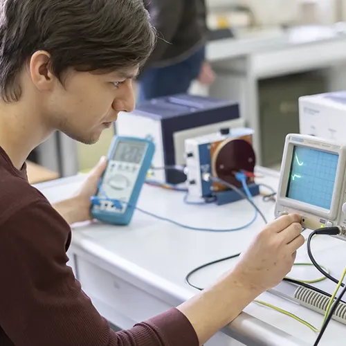
- Inspection and Testing: Use AOI (Automated Optical Inspection) and functional tests.
For beginners, hand soldering THT is a great start. Industry data shows SMT dominates, with automation reducing errors by up to 90%.
Common Mistakes in PCB Design and How to Avoid Them
Beginners often trip up, but knowing common mistakes can save headaches.
First, poor component placement: Crowding leads to heat issues. Solution: Group by function.
Second, inadequate trace widths: Thin traces overheat. Use calculators for proper sizing.
Third, ignoring signal integrity: Long traces cause noise. Keep them short.
- Forgetting DRC: Always run checks.
- Overlooking Power Planes: Add for stable supply.
- Bad Grounding: Use star or plane grounding.
Videos like “Top 5 Beginner PCB Design Mistakes” highlight these, emphasizing fixes for EMI and SI.


Trends in PCB Design and Assembly for 2025
Looking ahead, PCB trends in 2025 include miniaturization with HDI (High-Density Interconnect) for compact devices.
Flexible and rigid-flex PCBs are rising for wearables. Advanced materials like graphene enhance performance.
AI in design optimizes layouts, while 3D printing speeds prototyping. Sustainability is key, with green materials reducing e-waste.
The industry is shifting to eco-friendly practices, like using recyclable substrates.
How Panasia Solutions Excels in PCB Design and Assembly
At Panasia Solutions, our 25+ years of expertise make us leaders in PCB design and assembly. With global facilities in Dongguan, China, we offer end-to-end services, incorporating sustainable practices like eco-friendly materials.
We help beginners scale to production, ensuring quality through advanced tools and checks.
Start Your PCB Journey Today
This guide to PCB design equips you with the basics to build and assemble your own boards. As the market grows, mastering these skills opens doors.
Ready to prototype? Browse our services at Panasia Solutions or contact our team today for expert guidance.